中文詳細說明 : http://gc.digitw.com/Circuit/PCB-BY-TRANS.pdf
Make your own Microcontroller PCB using the Toner Transfer Method
As the electronics hobbyist one of knowledge that we have to be familiar with is how to make our own printed circuit board (PCB). Making our own simple single side PCB actually is not require a sophisticated technique and technology as you might think, instead most of the required materials is already available at your home. I’ve started make my first single side through-hole PCB for a simple two transistors astable multivibrator project using just a water proof marker and draw the PCB layout directly on the PCB copper surface.
On those days the CAD (computer aided design) for electronic schematic and PCB are expensive and it runs on the expensive computer hardware too. That is why most of the electronics hobbyist on those days rely only on the hand draw method and occasionally combine it with a special made sticker for drawing the IC parts.
Nowadays as the technology evolve making a decent quality home made single side PCB is become possible and easy. On this tutorial we are going to learn of how to make a through-hole single side PCB and later on use this home made PCB for many of the blog up-coming projects or you could simply use it for your project.
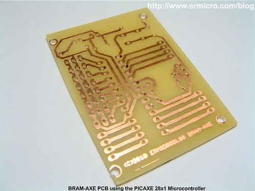
The BRAM-AXE Microcontroller Board
The BRAM-AXE microcontroller board is based on the PICAXE 28×1 microcontrollers from the Revolution Education Ltd (http://www.rev-ed.co.uk/picaxe). The PICAXE 28×1 microcontroller actually is based on the midrange 8-bit Microchip PIC16F886 microcontroller with preload PICAXE BASIC (Beginner’s All-Purpose Symbolic Instruction Code) interpreter firmware inside which is suitable for both beginners and advanced usage. Now let’s take a look at the BRAM-AXE microcontroller board electronic schematic which is specially designed to be used on this PCB tutorial.

The PICAXE 2×1 microcontroller has a build in program loader, therefore this board could be easily reprogrammed using the PICAXE programming editor by connecting the board COM/RS232 port to your computer serial COM/RS232 port or USB port with the USB to COM/RS232 adapter.

The PICAXE 28×1 microcontroller support up to 1000 lines of code, for more advanced application you could replace the PICAXE 28×1 microcontroller with the PICAXE 28×2 microcontroller which based on Microchip advanced 8-bit PIC18F2520 microcontroller which support up to 4000 lines of code.

For more information about the PICAXE microcontroller you could read my previous posted blog Introduction to the Embedded System with PICAXE microcontroller.
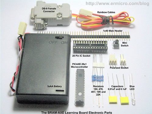
The following is the list of electronic parts required to assembly the BRAM-AXE board:
1. Resistor ¼ watt: 180 Ohm (1), 470 Ohm (1), 4K7 (1), 10K (1) and 22K (1)
2. Capacitor: 0.1 uF (1) and 0.01 uF (1)
3. One PICAXE 28×1 microcontroller
4. One 28 pin IC Socket
5. One mini switch button
6. One blue 3mm LED
7. One 2 pin polarized socket for the power supply
8. One 3 pin polarized socket for the COM/RS232
9. One COM/RS232 DB-9 female connector and cable
10. Optional USB to COM/RS232 adapter
11. One 1×40 male header
12. 3xAA battery holder and 3xAA alkaline battery for powering the board
The BRAM-AXE Board PCB Layout
The BRAM-AXE board schematic is created with EAGLE version 5.6.0 Lite Edition; it’s a freeware version of the powerful CAD software made by CADSOFT (http:// www.cadsoft.de) for creating electronics schema and generating the PCB layout. This following picture is the PCB layout generated by this software:

For the purpose of this tutorial I will not describe of how to use the EAGLE software, all of the EAGLE software project files and the PDF print out could download from BRAM-AXE PCB on this blog. You could visit the CADSOFT website above for more information and tutorial of how to use the EAGLE software for creating electronic schematic and generating the PCB layout from it.
Ok know let’s list down all the material required to make this BRAM-AXE board PCB:
1. A piece of glossy magazine paper, brochure, catalog for the toner transfer method medium.
2. Laser Printer with adequate toner for printing the PCB to the glossy magazine paper or you could also use a copy machine
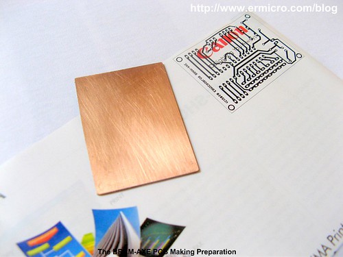
3. 60×45 mm Copper clad laminated printed circuit board (PCB)
4. Kitchen scrub with soap to wash the PCB
5. Hacksaw and sandpaper for cutting the PCB and smoothing
6. The house hold iron for doing the actual toner transfer from the glossy magazine paper to the PCB
7. Ferry Chloride for etching
8. Plastic container for etching and washing
9. A pair of disposal rubber hands glove and eyes protection goggle
10. Nail Polish Remover to remove the toner from the PCB
11. Water proof marker
12. Hand drill with 1mm and 3mm drill bits for drilling the through-hole PCB
The Toner Transfer Method
The toner transfer method is actually based on the same principal as the professional PCB making process, but instead of using the expensive photo film and photosensitive material to transfer the PCB drawing layout to PCB copper; we use the laser jet printer toner to do the job.

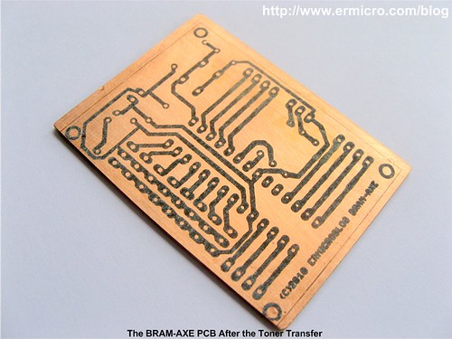
The laser jet printer toner actually contain a plastic material and not an ink as the deskjet printer does; therefore when we print this PCB drawing layout on a glossy paper, the black toner plastic material will be attached only on the surface of this glossy paper; by using enough hot from the house hold iron we could make this black toner plastic material melt and reattached to the PCB copper surface.
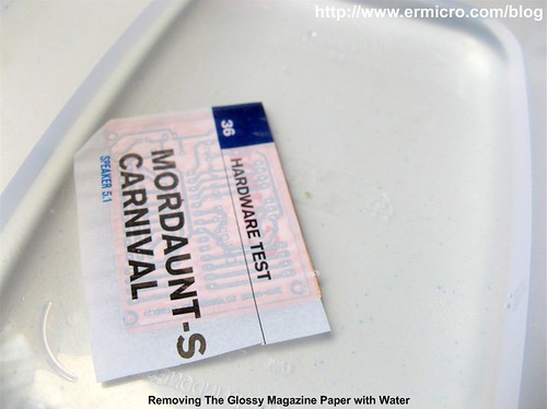
Now as the magazine glossy paper and the black toner plastic material attached to the PCB copper surface, we could easily remove the paper part by submerging it in the water; once the paper dissolve and become pulp what is left is the black toner plastic material on the PCB copper surface.
Using the etching process the uncovered area on the PCB copper surface will chemically react with the Ferry Chloride (FeCl3) solution and become dissolved but the covered area will not be dissolved as it being protected by the black toner plastic material. The last step is to remove this black toner plastic material using the nail polish remover and drill the board.
The Making of BRAM-AXE Board PCB
Now as you understand how this toner transfers method work; let’s make the BRAM-AXE board PCB.
The Preperation
- Cut the copper clad laminated PCB to 60×45mm size and smooth it’s surrounding with the sandpaper.
- Wash and scrub the PCB using the kitchen scrub and soap to remove any dirt and grease on the PCB copper surface
- Cut the glossy magazine paper to about half of A4 paper length size and full width of A4 paper size; try to use the paper with less printed image or letter on it, so you could easily examine the printed PCB layout. In fact you could use any glossy paper; but do not use the glossy photo paper as it hard to remove the glossy coating material on the PCB copper surface when the toner has been transferred; just safe it for printing your photo.
- Print it with the laser jet printer on the glossy magazine paper. The other alternative is to print it with other type of printer (e.g. deskjet printer) and use the real copier machine to copy the PCB layout to the glossy magazine paper because the copier machine use the same toner material as the laser jet printer. On this tutorial I used the HP LaserJet P1006 to print this PCB layout.
- When printing the PCB layout you could use the EAGLE software directly or you could use the PDF version of the PCB layout provided here.
The Toner Transfer Process
- Next aligned the glossy magazine paper so the printed PCB layout is facing toward the PCB copper surface and you could lock this paper corner with the tape so it won’t move. Cover the glossy magazine paper with another paper to protect it again the over heating (usually this glossy magazine paper is quite thin).
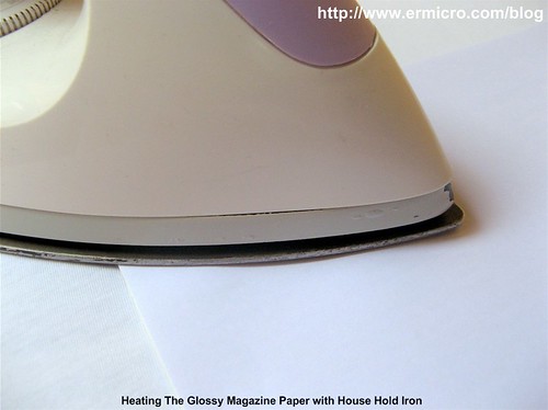
- Power on the house hold iron and set it to its maximum heat, let it become hot for a while.
- Pre-head the PCB copper surface for about 15 seconds, this will ensure the toner from the glossy magazine paper will transfer perfectly.
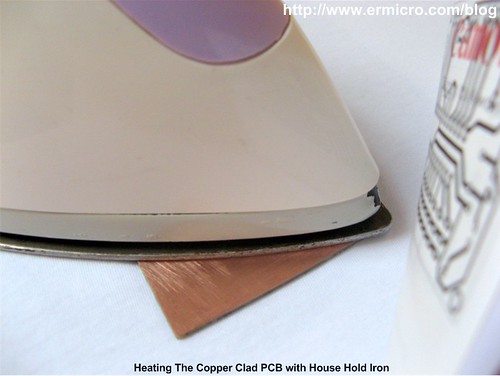
- Flip the glossy paper magazine toward the PCB precisely; apply pressure and move gently the iron on the top of the paper for about 45 second, make sure you cover the whole PCB layout. Wait until it become cold, do not remove it while it is hot as it could harm your hand and the black toner plastic material will not transfer perfectly to the PCB copper surface.
- Trim the glossy magazine paper so it has the same size as the PCB. Next immerse the PCB in the water and wait for a couple of minutes than gently pealing all the paper until it all being removed.
- Examine the PCB layout, and make sure all the connection is perfectly covered by the black toner. You could use the marker to repair the tiny un-perfectly covered area or you could repeat the whole process again by first removing all the black toner using the nail polish remover.
The Etching Process
- Prepare the etching solution in the plastic container by mixing four part of water with one part of Ferry Chloride (FeCl3) and it would be better to use the hot water about 40 to 50 centigrade degree because the chemical reaction will be faster at higher temperature.
- Make sure you are wearing the disposal rubber hand glove and the eye protection goggle when working with this Ferry Chloride solution because this chemical acid solution is very corrosive and poison; you should always take extra precaution when working with this Ferry Chloride solution. If you accidentally exposed with this acid solution, make sure you wash it with plenty of water and soap.
- Next immerse the PCB in the Ferry Chloride solution and gently move backward and forward the plastic container so the chemical solution could react with the PCB uncovered copper effectively. Keep watching until all the uncovered copper area becomes dissolved.
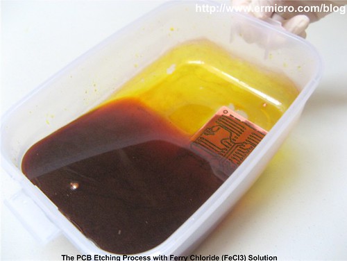
- Wash the PCB with plenty of water and soap; make sure you mix the Ferry Chloride solution with the water and soap solution to neutralize this remaining acid solution before you discard it. Usually the Ferry Chloride solution could only be used once, therefore use just enough amount as needed to etch your PCB. As a rule of thumb the acid solution area size should be a least twice as your PCB copper surface area size and the acid solution deep is about 10 mm to 20 mm.
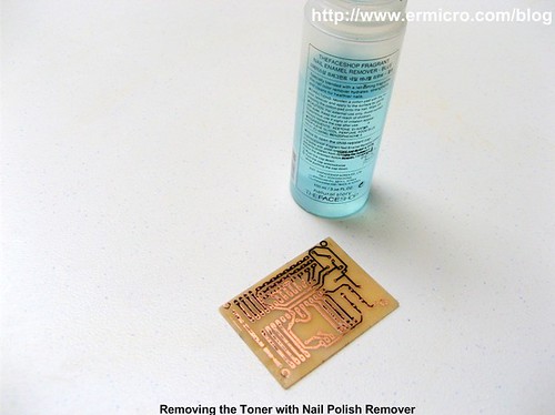
- The last process is to remove the black toner on the PCB copper surface with the nail polish remover (acetone); you could examine the black toner material while you are removing it and you will find out that it’s made from a plastic material.
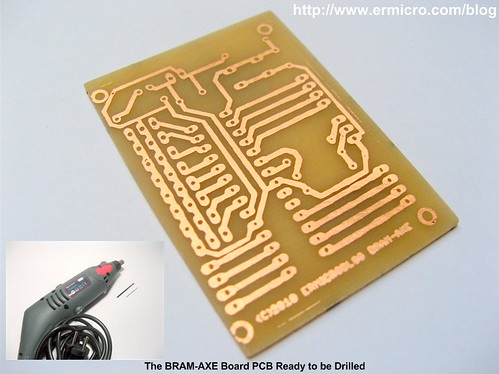
The Finishing
- Drill the PCB components hole with the 1mm drill bit size and the PCB stand off with the 3mm drill bit size. On this tutorial I’m using the general purpose hand drill to drill this PCB board.
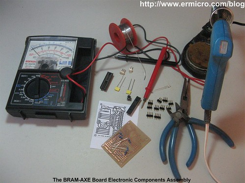
- Again wash and scrub the PCB with water and soap to remove any dirt and grease before you start to solder the electronic components on it.
To complete this tutorial we will assembly all the electronic components on the BRAM-AXE board, solder all the electronic components on it include the 28 pin IC socket and just leave it empty without the PICAXE 28×1 microcontroller.
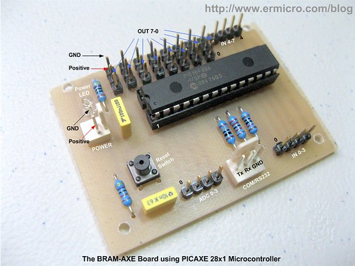
Now connect the 3xAA battery power to the board and make sure the power LED is lid; if not, disconnect the power and examine your 3xAA power connector make sure the positive and the ground pins are connect correctly to the board. Again examine all the electronics components if it ok, then disconnect the power and you could put the PICAXE 28×1 microcontroller on the 28 pin IC socket.
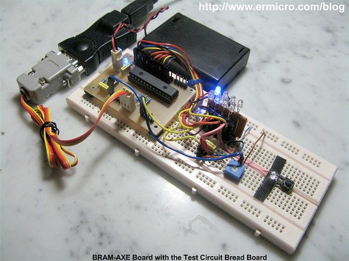
The BRAM-AXE Board PCB Test
After finish assembly all the electronic components now we are going to test this BRAM-AXE board I used this following test circuit to test both PICAXE 28×1 microcontroller input and output:

For the PICAXE 28×1 microcontroller output I used the SIL (single in line) LED as shown on my previous posted blog Single In Line (SIL) LED Display for your Microcontroller Based Project and for the PICAXE 28×1 digital input I used a mini push button switch and 10K trimport for the PICAXE 28×1 ADC (Analog to Digital Converter) input.
The following is the PICAXE BASIC program code for testing the BRAM-AXE board.
'***************************************************************************
'  File Name    : bram-axe.bas
'  Version      : 1.0
'  Description  : BRAM-AXE Board Testing Program
'  Author       : RWB
'  Target       : BRAM-AXE Learning Board - PICAXE 28x1
'  Intepreter   : PICAXE Firmware version A.6
'  IDE          : PICAXE Programming Editor Version 5.2.6
'  Programmer   : PICAXE Programming Editor Version 5.2.6
'  Last Updated : 03 January 2010
'***************************************************************************
' Use PICAXE 28x1 with 8 Mhz Internal Clock
#picaxe 28x1
SetFreq m8
' Assigned Variables
symbol adc_val = b0
symbol high_val = b1
symbol low_val = b2
symbol sign = b3
let pins = 000000 ' Reset all Output Pins
sign = 0             ' Default Running LED
main:
  ' Read Mini Switch on IN0
  if pin0 = 0 then
    sign=sign XOR 1
  endif

  ' Read 10K Trimport ADC Value on ADC0
  readadc 0,adc_val

  if sign = 1 then
    for high_val = 0 to 7
      low_val=high_val - 1
      low low_val
      high high_val

      pause adc_val
    next high_val

    for high_val = 6 to 0 step -1
      low_val=high_val + 1
      low low_val
      high high_val

      pause adc_val
    next high_val
  else
    let pins = %10101010
    pause adc_val
    let pins = %01010101
    pause adc_val
  endif

  goto main      ' Back to main loop
  end
' EOF: bram-axe.bas
Connect the DB-9 female COM/RS232 connector to your computer COM/RS232 port or you could use the USB to COM/RS232 adapter to connect the board to the computer USB port as I did. Now power the board and run the PICAXE Programming Editor, paste the above code and save it as bram-axe.bas.

Click the “Syntax” button in the PICAXE Programming Editor to check the PICAXE BASIC program syntax and if it ok than you could continue to compile and download the code to the board by choosing the “Program” button.
The eight LED blink pattern will change as you press the mini switch button, while the 10K trimport is used to adjust the eight LED blink speed as it take advantage of the PICAXE 28×1 microcontroller ADC capability to read the voltage value from the ADC 0 input.
Now you could enjoy this following video that shows all the BRAM-AXE Board PCB making process that we’ve been going through:
The Final Though
As you’ve learned through this tutorial, making a decent quality single side PCB actually is not a very difficult task; it’s not required a complex process like the conventional PCB making method (i.e. using the film and photosensitive method). The more you practice the whole process the more you gain the experiences from it.
Either you are an electronics hobbyist or a professional making your own PCB is one of the important knowledge that you should acquired; just imagine this situation one day in the middle of the night suddenly you get an idea of a very cool electronics circuit and you eagerly want to prototype this circuit as soon as possible; now your experiences in making the PCB become handy as you could make your own prototype circuit PCB right away.
沒有留言:
張貼留言
注意:只有此網誌的成員可以留言。